CMP
CMP
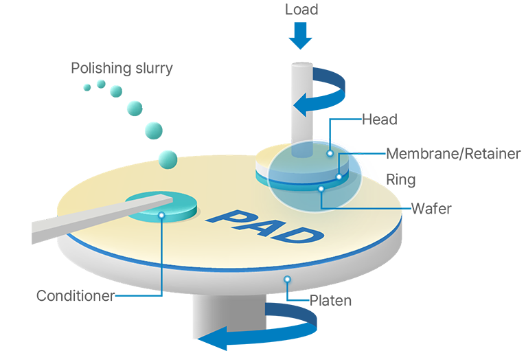
CMP PAD is a key material used in the Chemical Mechanical Planarization (CMP) process of semiconductor circuits and plays an essential role in polishing the surface of semiconductor wafers to flatten them while minimizing defects such as Scratch.
Features of KPX Electrochem CMP Pad
-
High Reproducibility
High reproducibility in removal rate and scratch/defect control across our pad products ensures uniform CMP process results.
-

Lifetime Stability
Optimization tuning for each CMP process for the physical properties/performance of the pad enables long lifetimes, which contributes to the customer's process cost reduction.
-
Customized Design
Leveraging advanced urethane synthesis technology, the company enables flexible tuning of material properties and delivers products tailored to customer needs through a wide range of pore formation technologies.
-
Simulating Customer Lines
We operate a customer-equivalent, production-grade CMP facility, enabling product recommendations backed by reliable demo test data.
KPX Electrochem CMP Pad Product Line-up
| Product |
Pore Tech |
STI |
Poly |
ILD/IMD |
Tungsten |
Copper |
Buffing |
| KONI |
Liquid |
|
|
|
O |
|
|
| KONIJ |
Gas |
|
|
|
O |
|
|
| IT series |
Hybrid |
O |
O |
O |
O |
O |
|
| KT series |
Microsphere
(VDC free) |
O |
O |
|
O |
O |
O |
| AT series |
O |
|
O |
O |
|
|
| LHB series |
Foaming |
|
|
|
|
|
O |
| Recycled Pad |
N/A |
O |
|
O |
O |
|
O |